A Working 8 bit CPU + Assembler
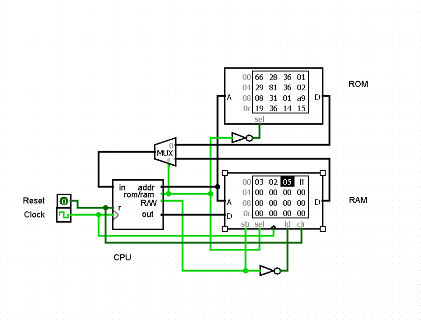
In this project, an 8-bit CPU was designed in the digital circuit simulator called Logisim. The CPU was built from logic-gates upwards and has its own instruction set and assembler. It currently also has a byte-code program loaded into its ROM, which adds the numbers at the 1st and 2nd memory addresses in RAM, displays the result into the 3rd memory address and then demonstrates branching by writing FF into the 4th address if the resulting sum is odd and 00 if it is even.
What is an 8-bit CPU?
8-bit CPU refers to that operates with a data width of 8 bits. The system can process and represent information using 8 binary digits or bits. This typically allows for a total of 256 different values to be represented, ranging from 0 to 255.
Download the article (.doc): CPUDescription.docx
Download the article (.pdf): CPUDescription.pdf
Feel free to download the source files of this project.
Download
Logisim: logisim-win-2.7.1.exe
Circuit design: CPU4CSoc.circ
Assembler: Assembler.py
Commands: ALUCMD.txt
How to Run?
The first step is to download and set up Logisim (https://www.cburch.com/logisim/). The next step is to download the appropriate files from either my website (gyularabai.com/cpu) or the GitHub (https://github.com/mrgyularabai/Logisim-CPU-8Bit), which should at minimum be the .circ file. Finally, open the file with Logisim, reset the memory (with the reset pin), enter the inputs into RAM and enable the clock ctrl + K.
Video explanation
Architecture
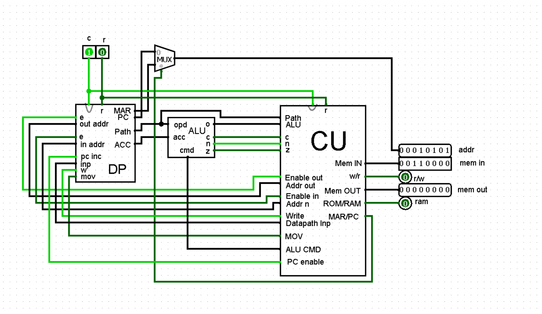
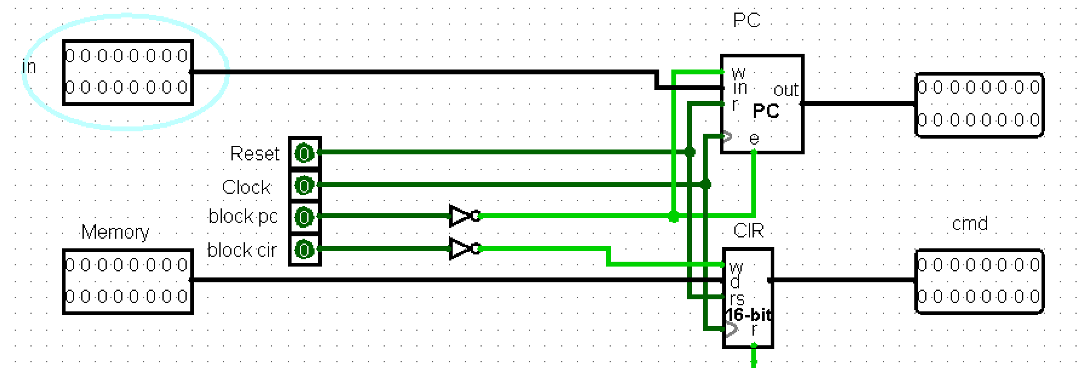
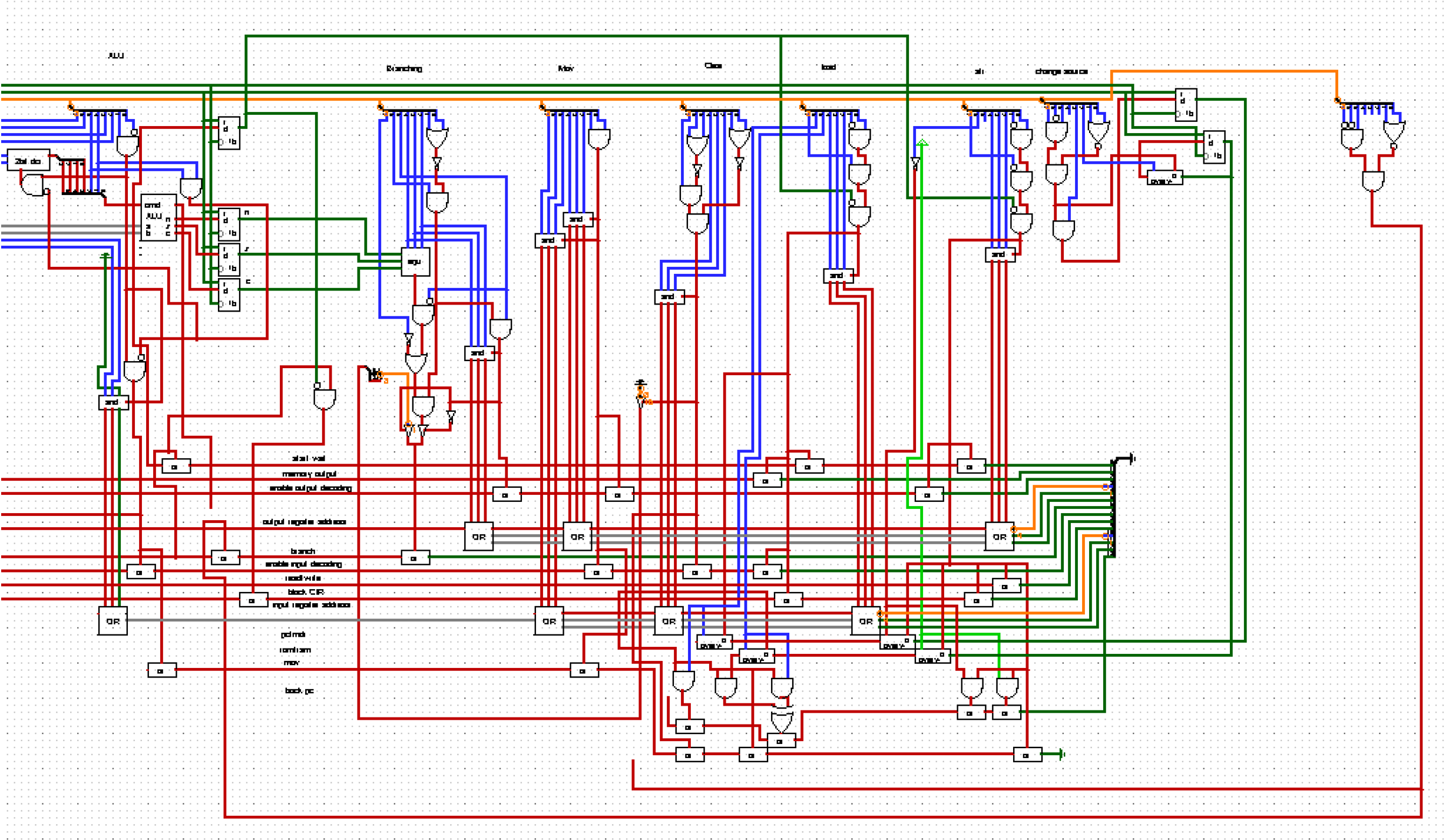
CPU
The CPU consists of three main parts: the ALU, the data path, and the control unit.
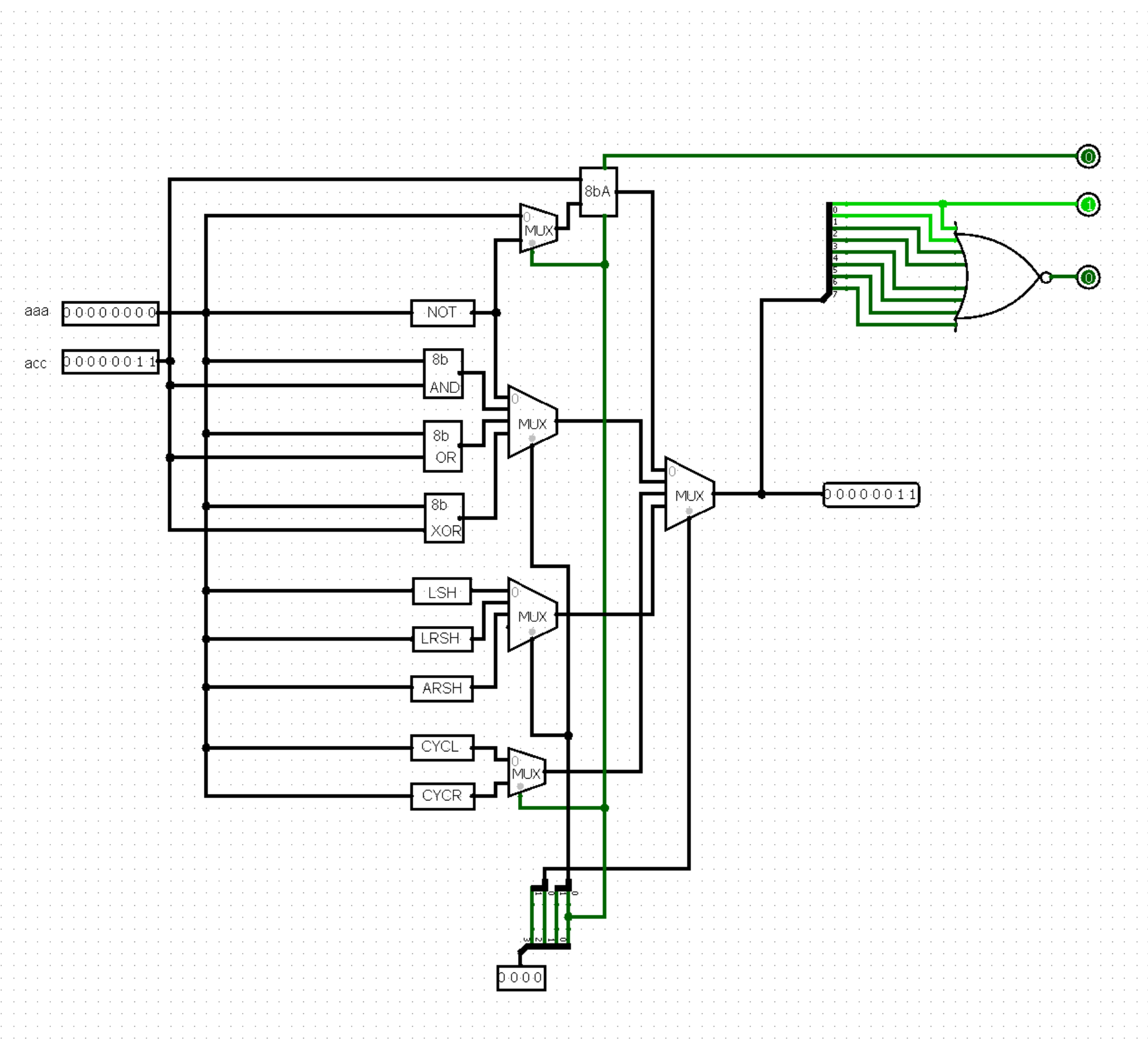
ALU
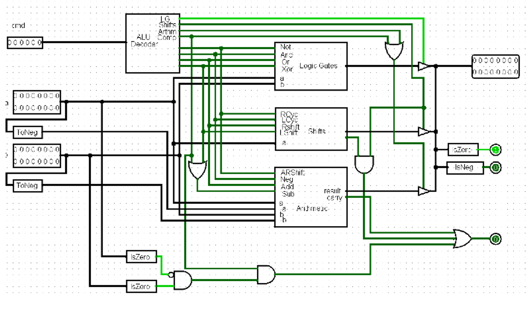
The arithmetic logic unit accepts two 8-bit buses and performs all operations on them (Addition/Subtraction, Shift Left, Shift Right, Arithmetic Shift Right, Cycle Left, Cycle Right, AND, OR, NOT, XOR), and a multiplexer selects which operation should be the output. It also updates the zero, carry, and negative registers if it performs a comparison operation.
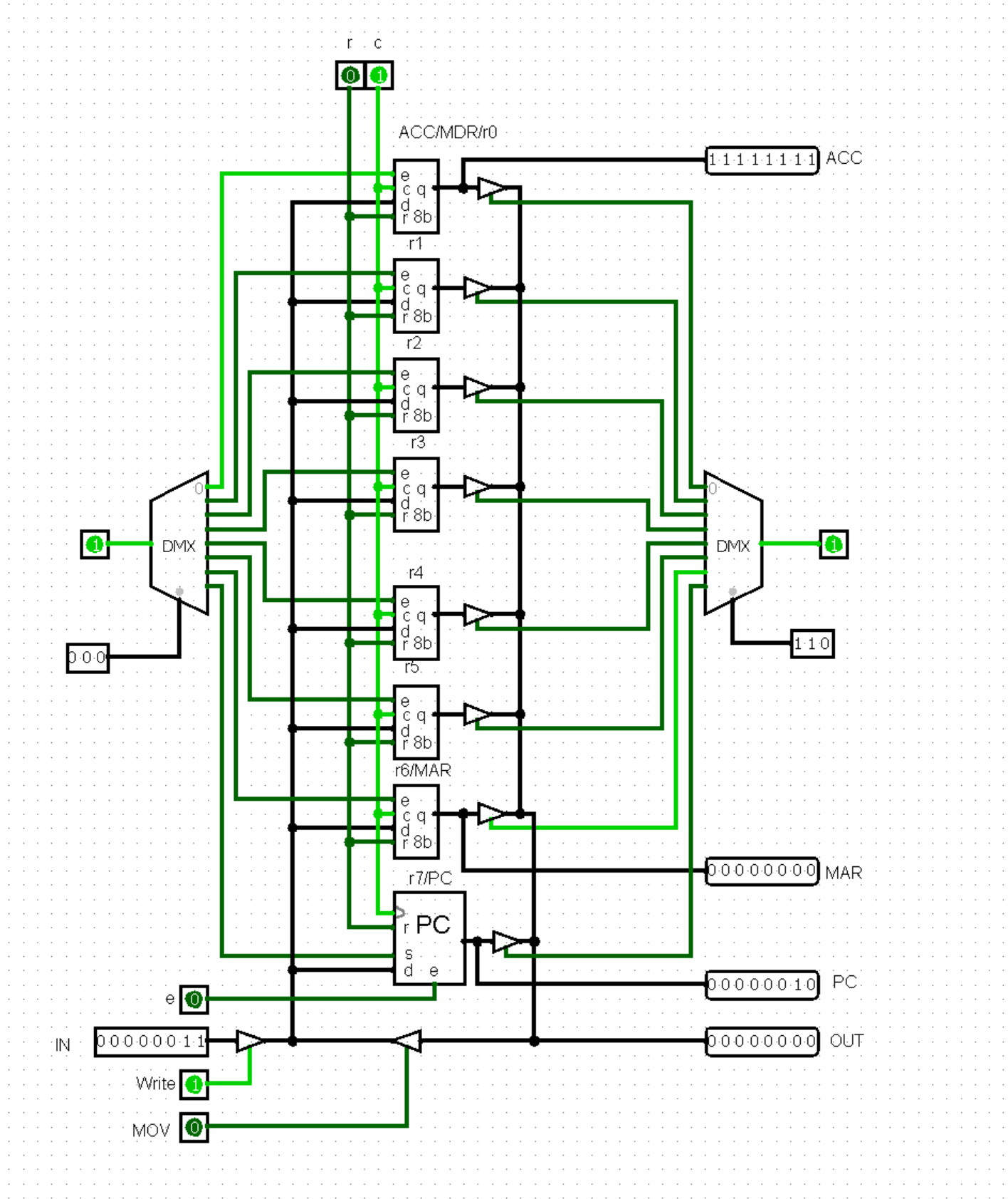
Data Path
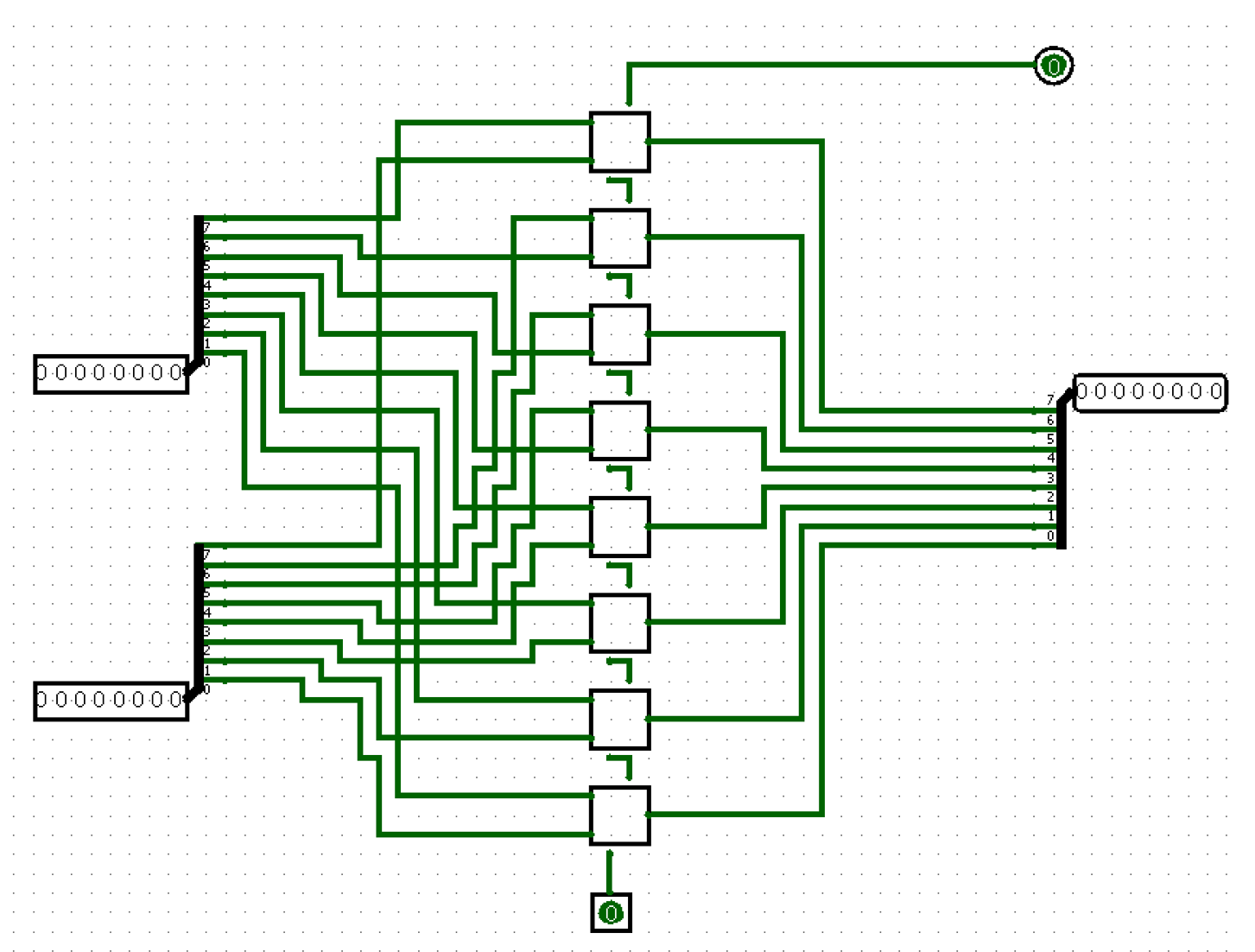
The data path contains 8 registers. Register 0 is the accumulator where all the ALU operations’ results are saved, and it is hardwired to be an operand of the ALU. Registers 1 through 5 are general purpose registers. Register 6 is the memory address register, which means load, store, and branch operations use this register when a memory address is needed as an operand. Finally, the program counter is register 7, which increments each clock cycle (given that the operation currently executed does not disable that). All these registers are connected to one central bus and whether they accept input from or write to that bus is determined by demultiplexers and a series of tri-state buffers.
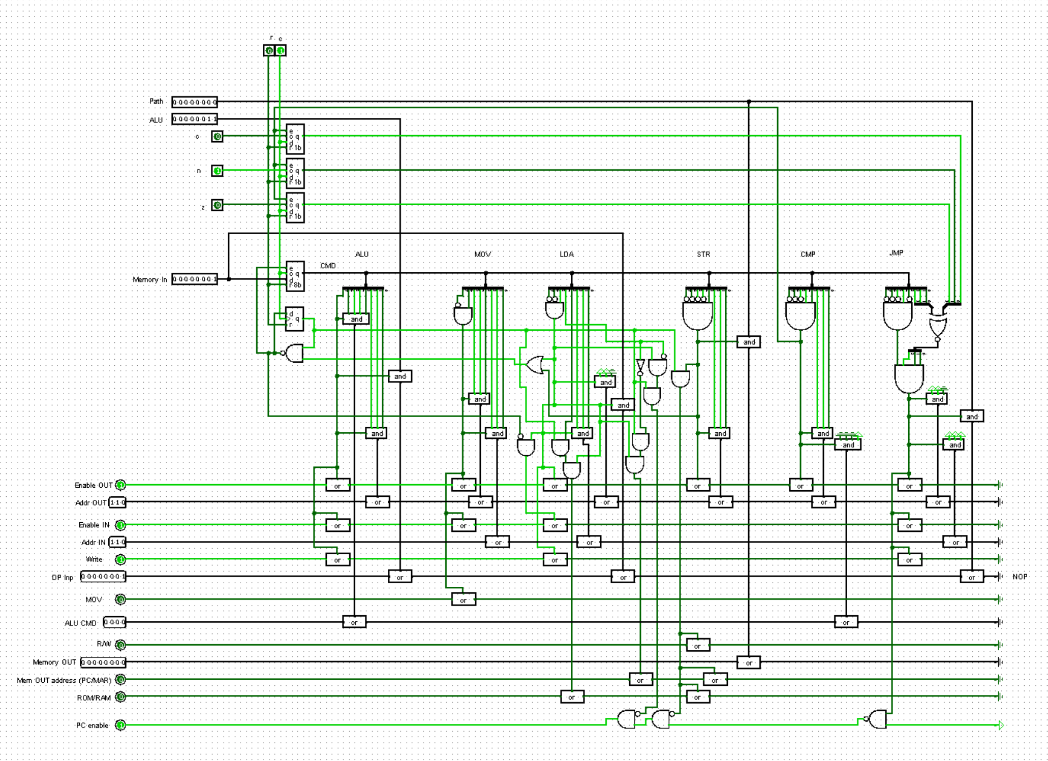
Control Unit
The control unit contains the current instruction register and accepts all the input and output pins in the entire CPU. It connects them or writes to them according to which operation is in the CIR. It also contains a few 1-bit registers to extend the duration of instructions like load or branching whilst the data is loaded or the next memory address is found.
Assembler and Instruction Set
The assembler fills in the correct fields in each byte (representing one instruction) based on what instruction is provided in human readable format. It then displays the HEX code that has to be entered into ROM.
The instruction set itself uses the first bit to indicate whether the operation is handled by the ALU or not and then at maximum 3 bits are reserved for one register as an operand (or 6 for two operands uniquely in the case of mov). The CMD.txt provides a more detailed description of the instruction set.
Test Program
Here is the test program roughly translated into its equivalent in C:
int main()
{
	//inputs may vary
	char a = 1;
	char b = 2;
	char c = a + b;
	if (c % 2 == 0)
		return 0;
	else
		return 256;
}
Motivation
I undertook this project to understand the inner workings of the CPU. I felt my knowledge was incomplete in this field despite it having been taught in the GCSE Compute Science curriculum. Even after taking the A-Level early, I was still not satisfied, and this is when I encountered drSigPro’s “8 bit Computer using Logisim” video. I was inspired to see whether I could construct something similar myself. However, I wanted my CPU to be more complex, supporting more operations. Therefore, I set off using the same software, but a different design. (Note my design itself takes little to no inspiration from the video other than the same choice of simulation software.)
Development
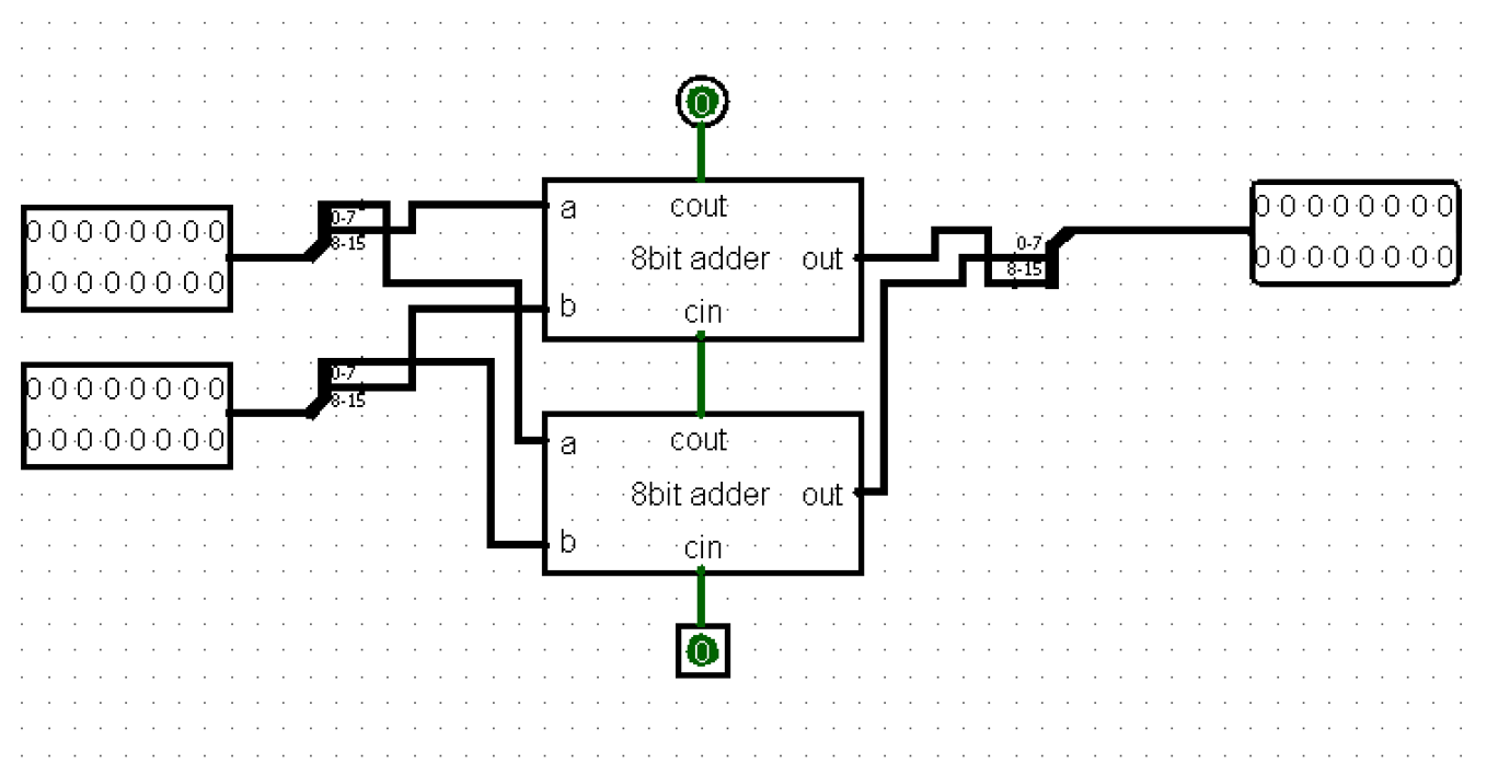
I started by developing the ALU of the CPU, not knowing much about the control aspect initially. I created a full adder and then instantly created an 8-bit adder by chaining 8 of them together. However, I did not consider the placement of pins and wiring very well, so it turned out to look a bit convoluted (but still functional). I further fumbled pin placement when I made a 16-bit adder for the a 16-bit PC, which led to very interesting connections to splitters.
Next, feeling confident, I targeted adding other operations. However, most of them did not require complex circuitry. Examples include shifts, which could be solved with splitters, and 8-bit wide logic gates that were already implemented into Logisim. To counter the mess that I caused earlier with the wires, I over-compensated in the other direction by making a separate module to contain everything in the ALU. This led to a very inefficient design (compare to the design in the Architecture section). The main faults were that I negated both inputs instead of reusing the addition circuitiry. I had also yet to learn of the multiplexer, which meant counteless attempts to use mutually exclusive tri-state buffers instead. However, worst of all, I ckeced whether any of the given operations would overflow instead of just for the addition operation as is required for comparisons.
Next, I designed the data path, which included 4 registers capable of being inputs for the ALU alongside the acc. The rest of the registers were grouped into pairs where the MAR was r4 and r5, and the PC was r6 and r7, both of which would act a 16-bit memory addresses for memory operations. Nonetheless, my inexperience led me to group the PC and CIR into one module, believing they would often be related by one operation or another.
Finally, in the first version of the CPU, I did not yet consider the control unit its own unit (I thought that it would be nigh on impossible to construct a module which comprehensively has access to all the connections required in the CPU). This led to one monolithic circuit containing all the circuitry, but roughly speaking, the right side could be considered the control unit, as is shown to the left.
The project did have unique features, however, such as being able to access 16-bit memory, and it could feed the CIR from both the RAM and ROM (there was one instruction to switch between the two), thus realizing the von Neuman architecture.
Eventually, however, I grew too ambitious, trying to upgrade it to a hyper-threaded 16-bit architecture. This failed on the wiring, because the datapath grew too complex without properly breaking the system down into submodules.
When I wanted to present what I had learnt in Computing Society, I did not want to present the CPU I had created above due to its convoluted and innefficient design. Therefore, I created the architecture presented in the earilier sections, which kept to a fully 8-bit design for simplicity, fully utlized the power of plexers and most importantly followed an instruction set I designed prior to creating the CPU. This meant I could get a both working and presentable CPU in the end.
FAQ
Are 8-bit processors still used?
Modernized versions of 8-bit CPUs are still very common in embedded systems.
Conclusion
Overall, this project resulted in two designs for an 8-bit CPU, and was a journey of improvement. I learnt how to organize circuits and connections in ways, which were both functional and easy to understand. However, most of all, I learnt how digital signals can form into a machine capable of general computation, and it all starts by assigning a meaning to a one or a zero.